 |
Source : AMD
|
AMD's Radeon RX 7000-series and the RDNA 3 architecture are slated to launch before the end of the year. AMD hasn't confirmed the name yet, but there's little reason to expect a change from the RX 6000-series model numbers. We're going to stick with RX 7000, though, until or unless we're proven wrong. These new GPUs will compete with the best graphics cards, and if the third time's the charm, AMD might even surpass Nvidia on GPU benchmarks hierarchy.
We've been reporting on various rumors and leaks for months, but we're finally close enough and have sufficient details that it's time to gather everything together into a single RDNA 3 and RX 7000-series hub. There are still plenty of unknowns, including price and a hard release date. Specifications will continue to fluctuate a bit while AMD finalizes its plans, but there's still plenty of data that we do know.
RDNA 3 / Navi 3x at a Glance
Up to 96 CUs / 12,288 shaders
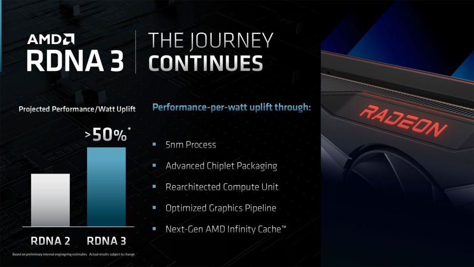
50% better performance per watt
Double the shader count per CU
GPU chiplet architecture
Up to 192MB of Infinity Cache
Launching before the end of 2022
AMD has not yet released details on the core specifications for its RDNA 3 GPUs. We do know AMD will be using "GPU chiplets" (see below), and it will also move at least some of the major building blocks to TSMC's N5 process node, but you should view the remaining details of RDNA 3 and RX 7000 as fuzzy, at best.
The existing RDNA 2 and RX 6000-series GPUs currently consist of four GPU designs spread out across a full dozen different graphics card models — and that's not counting integrated graphics solutions. We may eventually see a similar lineup from RX 7000, but we're only aware of three core GPUs at present: Navi 31, Navi 32, and Navi 33.
Logically, there will be multiple graphics card models using each GPU. AMD will also use GPU chiplets for the first time with RDNA 3, and the most credible sources indicate it will be breaking out the memory controllers and Infinity Cache from the main compute die. AMD will refer to the chips as the GCD (Graphics Chiplet Die) and MCD (Memory Chiplet Die), according to Angstronomics(opens in new tab). Note that the smallest die, Navi 33, will retain the same monolithic design as current GPUs.
Clock speeds are mostly placeholders for now. We don't expect AMD to walk back clocks relative to RDNA 2, and it's possible we'll see even higher clocks — perhaps the first GPU to break 3.0 GHz? For now, a conservative estimate of 2.5 GHz provides a rough guess at total compute. And compute... is insane.
With up to 12,288 GPU shaders each doing an FP32 FMA (Fused Multiply Accumulate) operation each cycle, that would potentially give the top model 61.4 teraflops of compute, and double that for FP16 workloads. Even the mid-tier chip would have a potential 38.4 teraflops, nearly double what the RX 6900 XT currently delivers. Which does make us wonder if perhaps these rumored specs are inflated, or if real-world throughput will be lower. We'll find out in the coming months.
Total memory bandwidth on the top models should increase by 50% relative to the RX 6950 XT. Again, it might be more than that, but we expect AMD to stick with "vanilla" GDDR6, and the supply of 18 Gbps chips seems reasonably plentiful. Real-world memory bandwidth will get a boost from the Infinity Cache, which for most models will decrease in size compared to RDNA 2. That could be offset by higher throughput or other tweaks to the design.
There are plenty of question marks in the table for now; frankly, we could put a question mark in nearly every cell and not feel too bad about it. Names, core counts, and other aspects are all unconfirmed at present, and the only thing we know for certain is that AMD will use TSMC's N5 node for at least some of the chiplets.
 |
| Source : AMD |
As we've seen with the past two generations of AMD hardware, AMD targets at least a 50% improvement in performance per watt with RDNA 3. While that might seem reasonably specific, it leaves plenty of wiggle room. For example, RDNA 2 delivered 50% better performance per watt than RDNA. Let's give some concrete examples of how that played out.
According to our GPU benchmarks hierarchy, the RX 6900 XT consumes 308W of power while delivering 130 fps at 1080p ultra, 106 fps at 1440p ultra, and 63 fps at 4K ultra. A lower-tier RX 6700 XT uses 215W and averages 96 fps, 71 fps, and 39 fps, while the RX 5700 XT consumes 214W while delivering 74 fps, 53 fps, and 29 fps at those same resolutions.
Do the math, and the 6900 XT provides a 22% to 50% improvement in performance per watt, while the 6700 XT only provides a 29% to 34% improvement. If we add in all the other RDNA and RDNA 2 GPUs as reference points, the potential spread for performance-per-watt improvements will become even wider.
The most reasonable assumption is that the top RDNA 3 chip will deliver a significant boost to performance compared to the current top RDNA 2 chip. Considering the 50% boost to memory bandwidth, a similar or even larger boost to compute performance seems reasonable. We'll probably see higher maximum power draw from the top model, presumably the RX 7900 XT. Lesser tier models might deliver more performance than the current generation cards while drawing less power. Your choice of resolution and setting will also impact the potential gains.
AMD has also made vague references to architectural improvements. While it hasn't confirmed this, we expect the ray tracing hardware will get a significant overhaul. Current RDNA 2 chips use the texture units to help with BVH traversal, whereas Nvidia and even Intel have dedicated BVH hardware. Adding such hardware along with a second ray/triangle intersection unit could greatly improve AMD's ray tracing performance. That could also contribute a lot to a metric showing a greater than 50% improvement in performance per watt.
One of the biggest architectural updates for RDNA 3 is something we've already mentioned — the move to GPU chiplets. There are a lot of good reasons for moving to multiple chiplets, though we're still curious about the overall net benefit, which mostly seems to be about reducing cost.
Current GPU designs are monolithic, meaning everything needed for the GPU to function comes from a single piece of silicon. Because of that, GPUs build in a lot of redundancy, and chips get sold in "harvested" configurations. Navi 21 was used in the 6950 XT, 6900 XT, 6800 XT, and 6800, with up to 80 compute units (CUs) or as few as 60 CUs.
Interestingly, the Navi 21 die also has eight 32-bit memory interfaces, but AMD didn't release any Navi 21 variants with fewer memory channels. The same mostly applies to Navi 22, Navi 23, and Navi 24 — memory and cache sizes seem to have been an all-or-nothing thing. Perhaps because the design didn't allow for it, though Navi 22 was used in the RX 6700 (non-XT) from Sapphire with a 160-bit interface instead of the full 192-bit interface.
With Navi 31 and 32, AMD will pull all of the memory interface and Infinity Cache blocks out of the main die and move them into separate dies. Each MCD will contain a 64-bit GDDR6 interface and a 16MB chunk of Infinity Cache. Actually, the MCDs will have the option to use 3D chip stacking with another 16MB die on top of the main MCD, so they can have either 16MB or 32MB of cache. All indications are that the 32MB MCDs with stacked cache will only be used on the halo graphics card model (RX 7900 XT or whatever it's called), but that could change over time. The MCDs will link with the GCD via AMD's Infinity Fabric, which will see some updates to the previous variants used in Ryzen CPUs.
Breaking out the Infinity Cache and GDDR6 memory interface has some clear advantages. Transistor densities scale best with logic circuits, less so with cache, and analog interfaces (i.e., for memory) scale the worst. The on-package Infinity Fabric links on both the GCD and MCDs still require some die space, but any faulty memory controllers or cache blocks will no longer be a problem — they just get tossed.
Meanwhile, the MCDs will be made on TSMC's existing N6 process, which costs less than the cutting-edge N5 (though N3 is coming soon), and die size won't even be a serious concern. Angstronomics claims that the MCDs will only be about 38mm square, meaning a 300mm N6 wafer should have enough room for about 1,600 MCDs, give or take. There would be no real difficulty in simply tossing every faulty chip rather than worrying about building in redundancies.
The GCDs for Navi 31 and Navi 32 also get to be smaller, and on the costlier N5 node, that could be very helpful. AMD could still get around 180 of the larger Navi 31 GCD per wafer or nearly 300 of the smaller Navi 32. And it can still use harvested chips with fewer compute units or even MCDs to create lower-tier products.
Had AMD stuck with monolithic designs, it likely would have ended up with Navi 31 using closer to 550mm square and getting maybe 100 chips per wafer. Since N5 wafers likely cost more than twice as much as N6, this should be an easy net win from a cost perspective. It also gives AMD more flexibility with cache sizes, at least on the higher-tier products. The stacked cache is only on the MCDs, leaving the GCD free to dissipate heat into the cooling setup — that's something 3D V-cache struggled with on its CPUs.
AMD will have plenty of other changes in the core architecture of RDNA 3. AMD has stated that it will have a rearchitected compute unit and optimized shader architecture, though the latter doesn't provide much in the way of detail.
One reasonably obvious change for the GPU shaders would be to cut down on the FP64 hardware. It's mostly there for compatibility reasons, and it costs die area. Nvidia's consumer GPUs have 1/32 the FP32 rate and have used that ratio for several generations now, while AMD has opted for 1/16 the FP32 rate. That's an easy fix.
The compute units will also be overhauled, and in an approach that looks similar to what Nvidia did with Ampere, we expect RDNA 3 CUs to have twice as many FP32 units. This will yield a massive boost to theoretical compute, as AMD will go from 80 RDNA 2 CUs and up to 5,120 GPU shaders to a maximum of 96 RDNA 3 CUs with 12,288 GPU shaders. Even if the real-world benefit doesn't scale directly with theoretical compute, this should greatly improve performance.
We've already mentioned that we expect AMD will also be tuning and tweaking the Ray Accelerators. Sharing the texture units with the BVH traversal hardware may have been okay for the first round of ray tracing hardware, but the second generation of Ray Accelerators needs to be better. DXR performance has been one of the few weak spots with RDNA 2, and while we're not yet at the point where ray tracing performance trumps rasterization performance, two years is plenty of time to incorporate some meaningful upgrades.
Finally, and again this comes from Angstronomics' RDNA 3 overview, AMD will reportedly add Opaque Random Export Order to the shaders. This is apparently another die-saving technique that eliminates some extra hardware like the Re-Order Buffer.
Overall, it's expected that the optimizations and improvements being made with RDNA 3 will result in significantly higher performance within a similar die size, even if the die were made on the same process node as RDNA 2. That's a big claim, and TSMC's N5 node(opens in new tab) should deliver up to a 1.8X improvement in density. RDNA 3 might even achieve such a lofty goal, given the removal of the GDDR6 interfaces and cache from the main GCD.


No comments